
A new era of computing power: a new era of integration from silicon light to edge computing
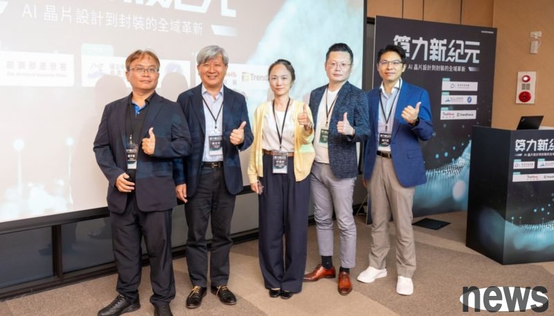
Research organization TrendForce held the "New Era of Computing Power - Global Innovation from AI Chip Design to Packaging" forum in Hsinchu on October 15, bringing together industry, government, academia and key partners in the industry chain to discuss AI chip design innovation, supply chain challenges and system-level integration trends. The event invited representatives from the Southern Chip Design Industry Promotion Base of the Industrial Development Administration of the Ministry of Economic Affairs, Synopsys Taiwan, Kneron Intelligence and Optical Technology to share topics and analyze the transformation of the semiconductor industry in the AI era from different perspectives.
The rise of new semiconductor clusters in the south—Kaohsiung New Bay AreaFor a long time, the center of Taiwan's high-tech industry has been concentrated in Hsinchu, while the south is actively replenishing upstream IC design capabilities. With the promotion and resource injection of the "Smart Electronic Chip Development Plan" of the Industrial Development Administration of the Ministry of Economic Affairs, it is accelerating the formation of another semiconductor cluster. The Southern Chip Design Industry Promotion Base of the Industrial Development Administration of the Ministry of Economic Affairs pointed out that Kaohsiung's "Asia's New Bay Area" has convenient transportation, dual advantages of port and air, and diverse demonstration sites. It also integrates resources such as space, technical support, resource injection, and market application to help companies quickly implement. She used Elan Electronics, PX Technology and Compal Computer as examples to illustrate the opportunities for companies to move south and the specific results of talent connection. In the future, Yawan will use IC × ICT as its dual main axes to drive more than 55 billion yuan in investment and high-skilled employment opportunities, and create a complete semiconductor ecological environment.
Low latency to high expansion—three major developments in optical communications in the futureChu Yuchao, vice president of TrendForce Research Department, pointed out that as the scale of AI applications continues to expand, high-speed optical communication has become a key driving force for the upgrade of AI server and data center architecture. At this stage, industry development is advancing in three major directions: Scale Up, Scale Out and Scale Across, which respectively correspond to transmission needs and technical bottlenecks under different distances and computing densities. Among them, the optical communication module market with Scale Out architecture as the core is expected to become the main battlefield for high-speed data interconnection and energy efficiency improvement in the next stage.
Scale-up (in the cabinet ≤10m): Pursue extremely low latency and high bandwidth, so it mainly uses electrical signal interconnection. Scale-out (≤2km in the computer room or campus): It uses light as the main body and uses technologies such as AOC, VCSEL or IM/DD to support high-speed transmission from 800G to 1.6T or even 3.2T. Scale-across (data center to data center): Mainly pluggable optical modules, taking into account both maintenance and scalability. When AI helps you design chips - design automation is no longer a dreamAs the amount of data and model scale continue to expand, chip design faces multiple challenges such as throughput, convergence, power consumption, and thermal management. Wei Zhizhong, strategy director of Synopsys Taiwan, pointed out that AI is not only a computing carrier, but also an assistant to designers. Through generative models and reinforcement learning, AI can help engineers significantly speed up parameter search and layout optimization, shorten design iteration time, and make the chip design process more flexible and efficient. Generative for RTL and automated workflow will become a trend, but at the same time, we must also pay attention to challenges such as quality verification, copyright management, and data governance to ensure the sustainability and reliability of automated design.
The development of Edge AI - striking a balance between performance, privacy and energy consumptionFaced with data privacy and latency issues, edge computing has become a mainstream trend that cannot be ignored. Chen Yuchun, assistant vice president of smart product marketing at Kneron, pointed out that the advantage of Edge AI is that it can complete inference locally, protect data sovereignty, reduce cloud costs and reduce delays, allowing the AI computing efficiency of PCs and devices to gradually surpass that of the cloud. In the future, algorithm and scheduling optimization will enable dynamic division of labor between GPU, NPU, CPU and DSP to optimize energy consumption and performance. However, he also reminded that the shortage of memory supply chain is still the biggest risk, especially the fluctuation of DDR and HBM production capacity, which will directly affect the performance performance and market rhythm of edge products.
MicroLED——Optoelectronic integration drives a new architecture for high-speed transmissionFang Yanxiang, Chief Operating Officer of Optoelectronics Technology, shared the latest breakthroughs in optoelectronic integration in the field of high-speed connections. He pointed out that silicon photonics technology is being deeply integrated with system packaging, paving the way for 1.6T, 3.2T or even higher bandwidth data transmission; while short-distance medium-to-high-speed connections are introducing MicroLEDs and new PDs and drivers, which can effectively reduce power consumption and costs. MicroLED has the characteristics of high brightness, fast response, high temperature resistance and arrayability. It is particularly suitable for short-distance high-speed applications ranging from a few centimeters to tens of meters. It can increase channel density and simplify heat dissipation design by "area conversion rate". In the future, the reduction of power consumption of the modulator and the mass production of 0° vertical coupling technology will become the key to the successful commercialization of optoelectronic packaging.
As AI drives deep changes in computing architecture and manufacturing models, semiconductors are showing a full-link development blueprint from AI-assisted design, optical interconnect technology to the implementation of edge AI systems. Facing the global competition for computing power, only by simultaneously improving design efficiency, strengthening data interconnection, optimizing end-side energy efficiency, and establishing robust supply chain resilience can Taiwan's industry continue to lead in the next wave of technology. The rise of southern settlements will become a new driving force for regional balance and the diffusion of innovation energy.
Recommend News
-

TSMC’s second wafer fab in Kumamoto, Japan will start construction, and the Gove
-
The gross profit is only 4%, but you still have to grab it! Qualcomm’s AI PC gam
-
AMD refers to the X3D processor burn problem, which is all the motherboard manuf
-

Alibaba AI chips are comparable to NVIDIA H20! Pingtou Ge was adopted by China C