Transfer the Taiwan Electric Network to post heroic posts to solve the problem of silicon intermediary layer and loading plate heat dissipation with 12-inch SiC
Silicon carbide (SiC) is expected to become a new outlet for Taiwanese manufacturers! As AI computing brings higher heat load, existing heat dissipation materials have been difficult to meet demand, resulting in a decline in chip performance. The semiconductor industry has been reported, and TECHN is publishing heroic posts, calling on equipment manufacturers and compound semiconductor-related manufacturers to participate, and plans to apply 12-inch single crystal silicon carbide to heat dissipation plates to replace traditional aluminum oxide, blue stone substrates or ceramic substrates.
In the past, silicon carbide was mainly used in power devices, vehicle and energy storage fields, and has now entered a new development stage. For example, in AR smart lens (AR Lens) lenses and high-level 3D IC packaging, silicon carbide is needed as a heat dissipation material, especially in the heat dissipation plate.
Among them, there are two possible directions for silicon carbide applications in 3D IC packaging. The first is the heat dissipation plate, which will be tested with "conductive SiC" first; the next stage may introduce semi-infrared SiC in the silicon interposer.
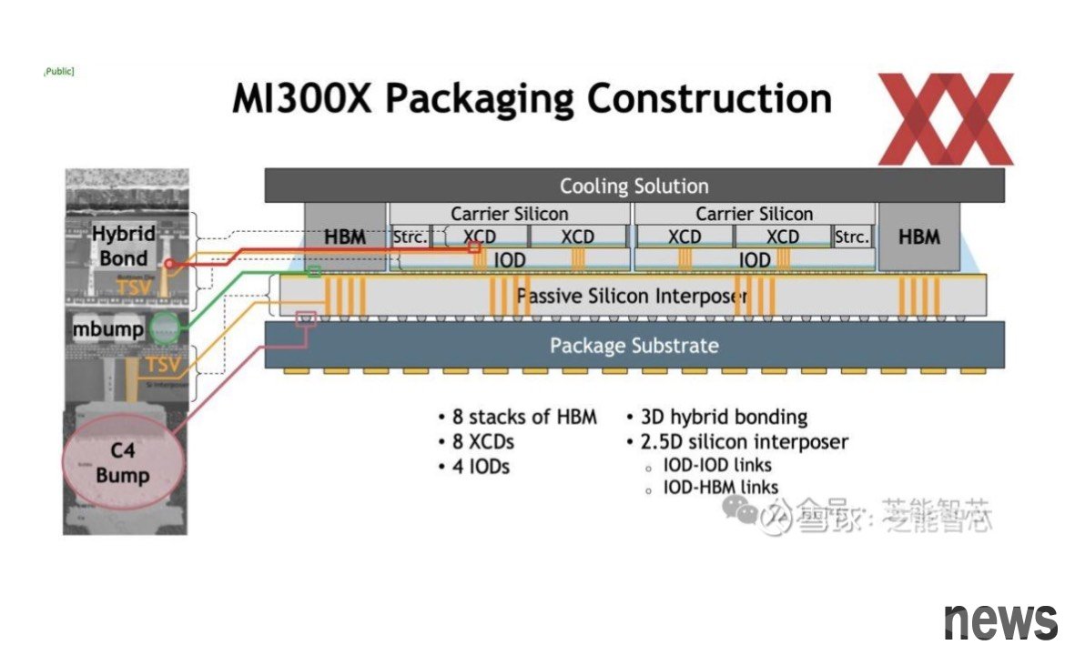
▲ As a heat-dissipating loader, it may be a first attempt to replace the Carrier Silicon part of the picture. (Source: Snowball, Zhineng Intelligent Core)
From the material characteristics, the thermal conductivity (K value) of silicon carbide is only as high as that of diamonds. The heat conductivity of ceramic substrates is about 200~230 W/mK, while silicon carbide can reach 400 W/mK, or even close to 500 W/mK. For high computing needs of data centers and AI, it can meet heat dissipation needs better than traditional ceramics. However, from the perspective of heat dissipation, diamond is still the ideal final material, but to achieve the 12-inch crystal round specification, the cost is too high and the technology is not yet mature.
Silicon carbide is mainly divided into conductive type (N type) and semi-infrared type. The N-type is translucent in yellow, while the semi-infinite shape is nearly fully transparent. Supply chain sources revealed that 6-inch SiC wafers are still mainstream and 8-inch is the future development direction. If the 12-inch SiC required by TECHNOLOG is used as an intermediary layer, the requirements for structural defects are not as strict as traditional SiCs, but the key to the intermediary layer is cutting technology. If the cutting technology is not good, the surface of the silicon carbide will be wavy and cannot be used for advanced packaging.
However, is this related to CoWoS next-generation extended technology CoPoS or CoWoP? Currently, only knows that SiC can be used as a heat dissipation material for NTD. Industry insiders believe that the application of silicon carbide will vary according to different packaging technologies, and there may be multiple development routes in the future. There is also a direction to try to apply silicon carbide on PCBs, but the most obvious application is still related to AI.
Extended reading: Resonac established an advanced packaging technology alliance to attack square substrate intermediary equipment Fujitsu launches advanced optical tests in Silicon Valley to attack AI data center business